


SpaceX's Terafab semiconductor complex could single-handedly double the global wafer-fab equipment market over five years.
SpaceX's Terafab semiconductor complex could single-handedly double the global wafer-fab equipment market over five years.
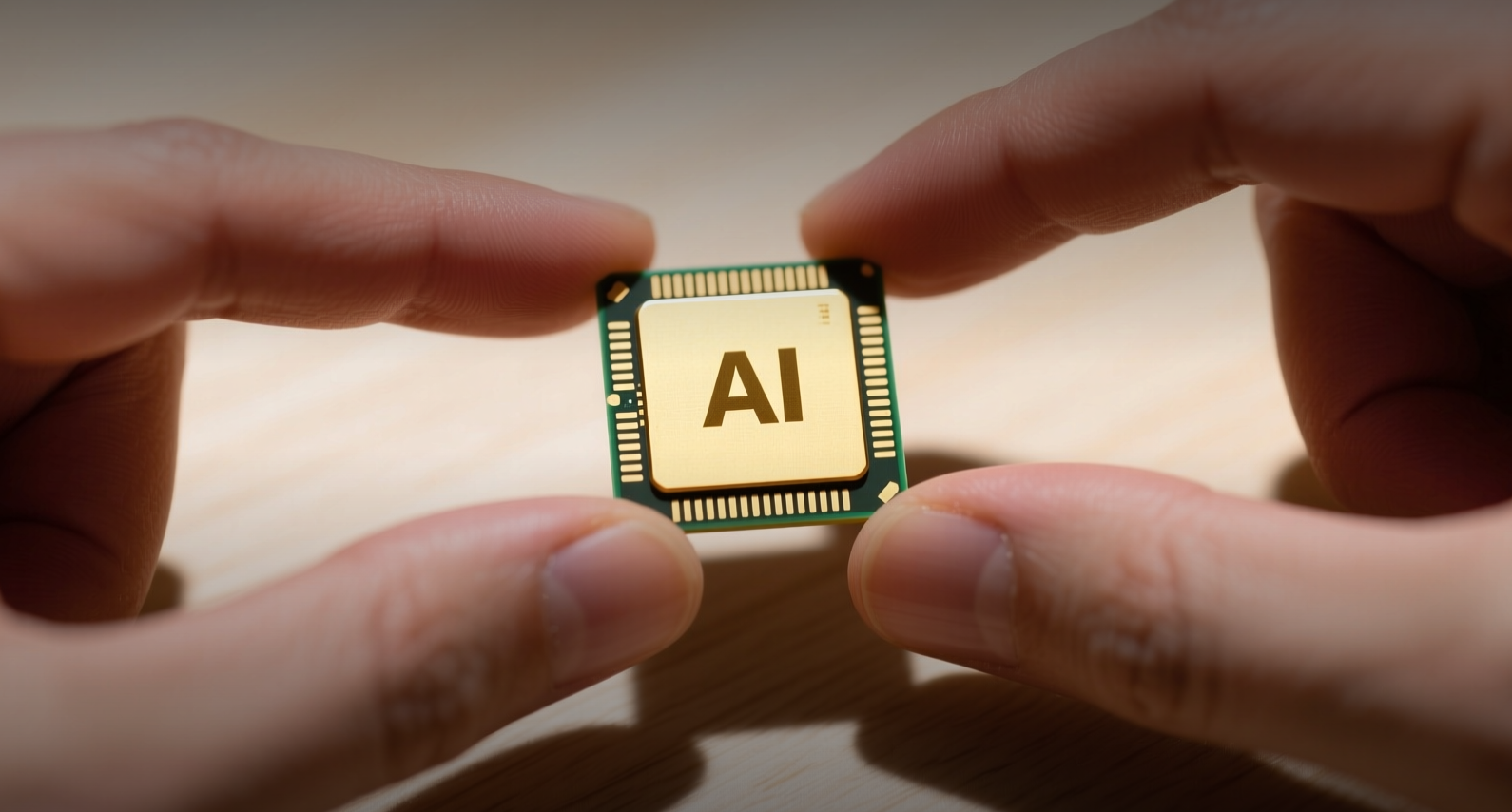
SpaceX's Terafab semiconductor complex could single-handedly double the global wafer-fab equipment market over five years.
SpaceX plans to spend about $135 billion on wafer-fab equipment for its Terafab project over the next five years, roughly matching the entire global market for such tools this year, according to UBS.
"The Terafab represents a new demand source the size of TSMC," Tim Arcuri, UBS analyst who initiated coverage of SpaceX with a buy rating, said in a July 7 note. "This will be a major theme in upcoming earnings seasons as construction gets under way."
SpaceX's AI-focused business is expected to devote about $1.1 trillion toward capital expenditures over five years, with roughly 20 percent — about $225 billion — allocated to the Terafab. Applying the industry-standard 60 percent conversion rate for wafer-fab equipment, that translates to $135 billion in tool spending, Arcuri estimated. The facility has already placed about $5 billion in equipment orders for a pilot line expected in 2027, with spending projected to reach $10 billion in 2028 and exceed $50 billion annually by 2030 or 2031.
If realized, the Terafab would make SpaceX a buyer of chip-making equipment on par with Taiwan Semiconductor Manufacturing Co., which builds most of the world's advanced chips. The spending trajectory could push the global wafer-fab equipment market toward $300 billion by 2029, Arcuri said. For equipment suppliers including Applied Materials, KLA Corp. and Lam Research, the Terafab represents a multi-year structural demand driver that could lift the entire sector's addressable market.
Elon Musk first unveiled the Terafab concept in March, arguing that existing foundries — including TSMC, Samsung and Micron — cannot expand fast enough to meet SpaceX's demand. Current global fab output for AI compute equals only about 2 percent of what SpaceX requires, Musk said at the time. The company plans to manufacture two chip categories: edge inference processors for its Optimus humanoid robots and high-power chips optimized for space environments. Musk estimated ground-based compute demand at 100 to 200 gigawatts annually, while space-based compute could reach about 1 terawatt.
The Terafab's design calls for a fully vertical integrated semiconductor complex under one roof — mask shop, leading-edge logic and memory fabrication, advanced packaging and testing — enabling a rapid design-to-manufacturing feedback loop. SpaceX has filed tax abatement requests in Grimes County, Texas, showing an initial semiconductor fab investment of $55 billion, with potential expansion to $119 billion if all phases are completed. That would support roughly 80,000 wafer starts per month of memory capacity and two logic fabs of about 20,000 wafer starts per month each, plus mask-making and back-end packaging lines.
Intel's Role and the Memory Question
Intel is in discussions with SpaceX about a technology licensing arrangement similar to the historical IBM-AMD framework, according to UBS. Under such a deal, Intel would provide process recipes, manufacturing intellectual property, PDK design rules and tooling know-how while retaining underlying technology ownership and collecting licensing fees. If the Terafab pilot line proves successful, Intel's "Ohio One" facility could be folded into the project as a joint venture, the report said. Conversely, if the Terafab fails to achieve independence, SpaceX's incentive to invest further in Intel would increase.
On the memory side, Musk has identified memory chips as a Terafab production target, but the source of memory intellectual property remains unclear. Existing memory suppliers have limited incentive to license core IP to a potential competitor. However, the report noted that a successful Terafab memory operation could pressure Korean manufacturers to accelerate front-end memory fab construction in the US — Samsung already holds ample land for expansion at its Taylor, Texas site, while Micron and SK Hynix are also monitoring the situation.
Investment Impact
For semiconductor equipment makers, the Terafab represents a multi-year demand driver regardless of its ultimate form. Applied Materials, KLA and Lam Research — which produce the inspection, metrology and etching tools needed for advanced chip fabrication — stand to benefit most directly from the projected $135 billion in equipment spending. ASML, the Dutch supplier of extreme ultraviolet lithography machines essential for leading-edge nodes, would also be a key beneficiary, though the company was not named in the UBS report. Teradyne, which makes chip-testing equipment, could see incremental demand as the Terafab's packaging and test operations scale.
The broader implication for investors: the wafer-fab equipment market, currently valued at roughly $135 billion annually, could nearly double in size within five years if the Terafab spending materializes as projected. Equipment suppliers trading at 20x to 25x forward earnings could see multiple expansion as the market reprices for a structurally larger total addressable market. The Terafab's construction timeline and equipment order cadence will be a key theme in semiconductor earnings calls over the coming quarters.
This article is for informational purposes only and does not constitute investment advice.
